STM32 OV2640 Save
Probably the best library for OV2640 camera on STM32 platform
Project README
Fully implementation library support OV2640 camera on STM32 platform
🚀 Features
Support for resolutions:
- 160X120px,
- 320X240px,
- 640X480px,
- 800x600px,
- 1024x768px,
- 1280x960px,
Added support for extra special effects:
- brightness,
- saturation,
- contrast,
- light mode,
- special effect such as: antique, bluish, greenish, reddish, black & white style, negative, Negative with black & white style and normal view.
Support for libjpeg library. Branch with example: https://github.com/SimpleMethod/STM32-OV2640/tree/Imageoptimization
Code optimization, now requires 10 times less space in buffer than before!
📚 Documentation
The maximum size of the data buffer is 65535 bytes and this is also the maximum size of a single DCMI read. For higher resolutions, you must use the circular buffer and write own implementation in HAL_DCMI_IRQHandler. XCLX is actually the clock output from the MCU (RCC_MCO_1). The minimum speed is around 27MHz, but as high as possible is recommended for correct functioning.
Pin configuration:
| PERIPHERALS | MODES | FUNCTIONS | PINS |
|---|---|---|---|
| DCMI | Slave 8 bits External Synchro | DCMI_D0 | PC6 |
| DCMI | Slave 8 bits External Synchro | DCMI_D1 | PC7 |
| DCMI | Slave 8 bits External Synchro | DCMI_D2 | PC8 |
| DCMI | Slave 8 bits External Synchro | DCMI_D3 | PC9 |
| DCMI | Slave 8 bits External Synchro | DCMI_D4 | PE4 |
| DCMI | Slave 8 bits External Synchro | DCMI_D5 | PD3 |
| DCMI | Slave 8 bits External Synchro | DCMI_D6 | PE5 |
| DCMI | Slave 8 bits External Synchro | DCMI_D7 | PE6 |
| DCMI | Slave 8 bits External Synchro | DCMI_HSYNC | PA4 |
| DCMI | Slave 8 bits External Synchro | DCMI_PIXCLK | PA6 |
| DCMI | Slave 8 bits External Synchro | DCMI_VSYNC | PG9 |
| I2C1 | I2C | I2C1_SCL | PB8 |
| I2C1 | I2C | I2C1_SDA | PB9 |
| RCC | BYPASS Clock Source | RCC_OSC_IN | PH0/OSC_IN |
| RCC | BYPASS Clock Source | RCC_OSC_OUT | PH1/OSC_OUT |
| RCC | Crystal/Ceramic Resonator | RCC_OSC32_IN | PC14/OSC32_IN |
| RCC | Crystal/Ceramic Resonator | RCC_OSC32_OUT | PC15/OSC32_OUT |
| RCC | Clock-out-1 | RCC_MCO_1 (DCMI_XCLX) | PA8 |
| SYS | Serial Wire | SYS_JTCK-SWCLK | PA14 |
| SYS | Serial Wire | SYS_JTMS-SWDIO | PA13 |
| SYS | SysTick | SYS_VS_Systick | VP_SYS_VS_Systick |
| USART3 | Asynchronous | USART3_RX | PD9 |
| USART3 | Asynchronous | USART3_TX | PD8 |
| GPIO | Output | CAMERA_RESET | PG0 |
| GPIO | Output | CAMERA_PWDN | PG1 |
| GPIO | EXTI13 | USER_Btn | PC13 |
DCMI configuration:
| OPTION | VALUE |
|---|---|
| Pixel clock polarity | Active on Rising edge |
| Vertical synchronization polarity | Active Low |
| Horizontal synchronization polarity | Active Low |
| Frequency of frame capture | All frames are captured |
| JPEG mode | Enabled |
I2C configuration:
| I2C Speed Mode | Standard Mode |
|---|---|
| I2C Speed Frequency (KHz) | 100 |
| Rise Time (ns) | 0 |
| Fall Time (ns) | 0 |
| Coefficient of Digital Filter | 0 |
| Analog Filter | 0 |
| Timing | 0x1060669A |
| Clock No Stretch Mode | Disabled |
| General Call Address Detection | Disabled |
| Primary Address Length selection | 7-bit |
| Primary slave address | 0 |
USART configuration:
| OPTION | VALUE |
|---|---|
| Baud Rate | 115200 |
| Word Length | 8 Bits(including Parity) |
| Parity | None |
| Stop Bits | 1 |
| Coefficient of Digital Filter | 0 |
| Data Direction | Receive and Transmit |
| Over Sampling | 16 Samples |
| Single Sample | Disable |
| Auto Baudrate | Disable |
| TX Pin Active Level Inversion | Disable |
| RX Pin Active Level Inversion | Disable |
| Data Inversion | Disable |
| TX and RX Pins | Swapping |
| Overrun | Enable |
| DMA on RX Error | Enable |
| MSB First | Disable |
DMA configuration:
| DMA request | Stream | Direction | Priority |
|---|---|---|---|
| DCMI | DMA2_Stream1 | PeripheralTo Memory | Very High |
| USART3_TX | DMA1_Stream3 | Memory To Peripheral | Very High |
DMA2_Stream1 DMA request settings:
| OPTION | VALUE |
|---|---|
| Mode | Circular |
| Use fifo | Enable |
| FIFO Threshold | Full |
| Peripheral Increment | Disable |
| Memory Increment | Enable |
| Peripheral Data Width | Word |
| Memory Data Width | Byte |
| Peripheral Burst Size | Single |
| Memory Burst Size | Single |
DMA1_Stream3 DMA request settings
| OPTION | VALUE |
|---|---|
| Mode | Normal |
| Use fifo | Enable |
| FIFO Threshold | Full |
| Peripheral Increment | Disable |
| Memory Increment | Enable |
| Peripheral Data Width | Byte |
| Memory Data Width | Byte |
| Peripheral Burst Size | Single |
| Memory Burst Size | Single |
NVIC configuration
| Interrupt Table | Enable | Preenmption Priority | SubPriority |
|---|---|---|---|
| Non maskable interrupt | true | 0 | 0 |
| Hard fault interrupt | true | 0 | 0 |
| Memory management fault | true | 0 | 0 |
| Pre-fetch fault, memory access fault | true | 0 | 0 |
| Undefined instruction or illegal state | true | 0 | 0 |
| System service call via SWI instruction | true | 0 | 0 |
| Debug monitor | true | 0 | 0 |
| Pendable request for system service | true | 0 | 0 |
| System tick timer | true | 0 | 0 |
| DMA1 stream3 global interrupt | true | 0 | 0 |
| USART3 global interrupt | true | 0 | 0 |
| DMA2 stream1 global interrupt | true | 0 | 0 |
| DCMI global interrupt | true | 0 | 0 |
| PVD interrupt through EXTI line 16 | unused | ||
| Flash global interrupt | unused | ||
| RCC global interrupt | unused | ||
| I2C1 event interrupt | unused | ||
| I2C1 error interrupt | unused | ||
| EXTI line[15:10]interrupts | unused | ||
| FPU global interrupt | unused |
📚 Example use
1. Receive the data using a terminal or other software, default speed is set to 115200 baud.
2. Save the data dump to a file.
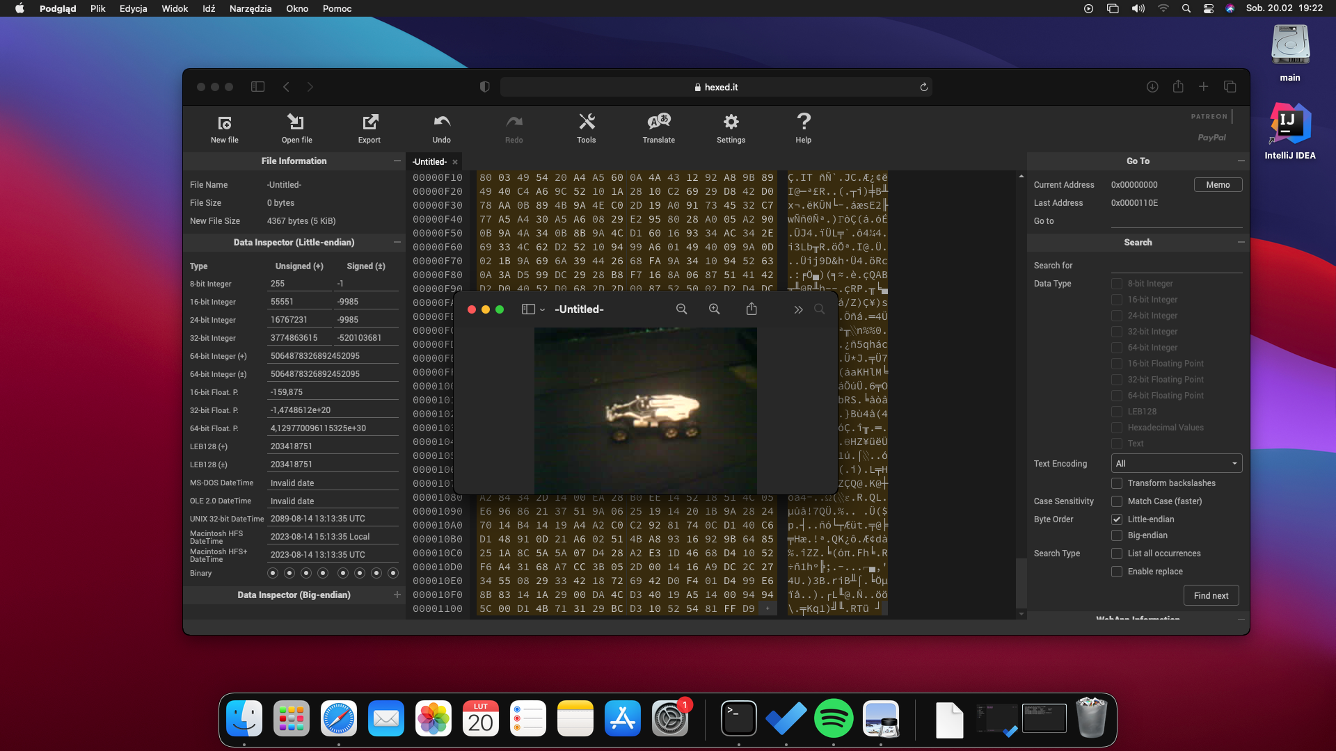
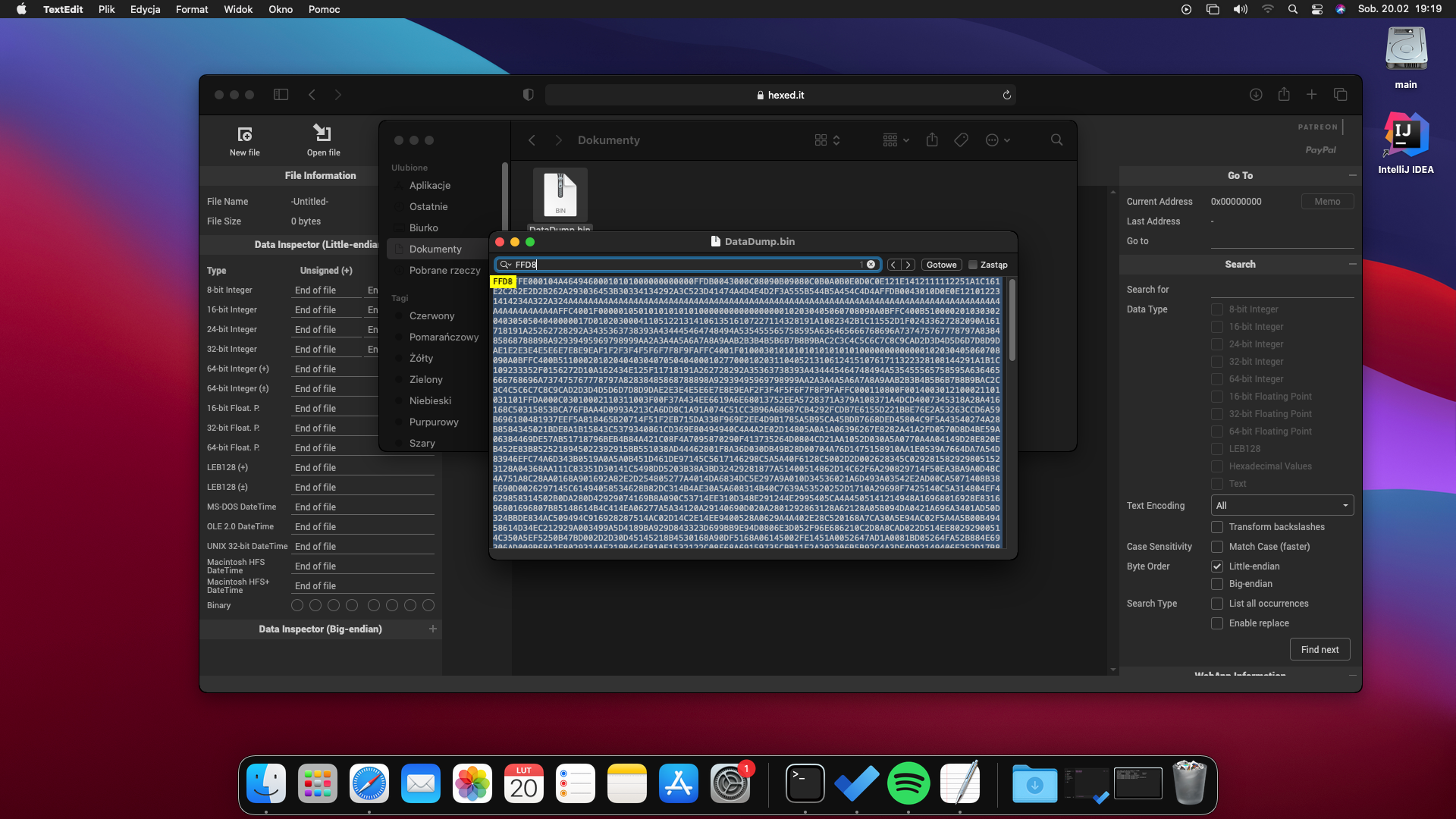
3. Open the file and search for the beginning of the JPEG header, it must be FFF8 value.
4. In the opened file search for the end of the data, this must be FFD9 value.
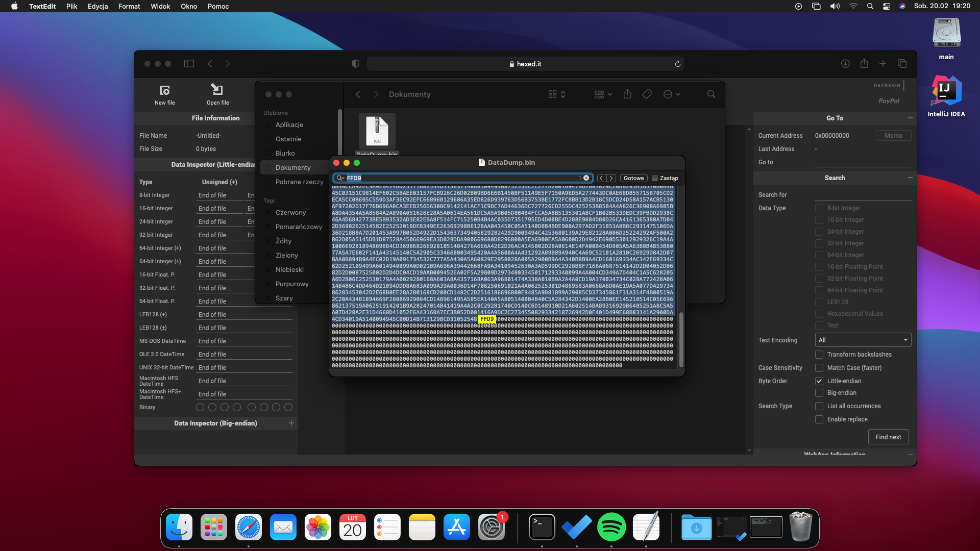
5. Open the hexadecimal editor. The example uses https://hexed.it/ and copy the data from the data dump.
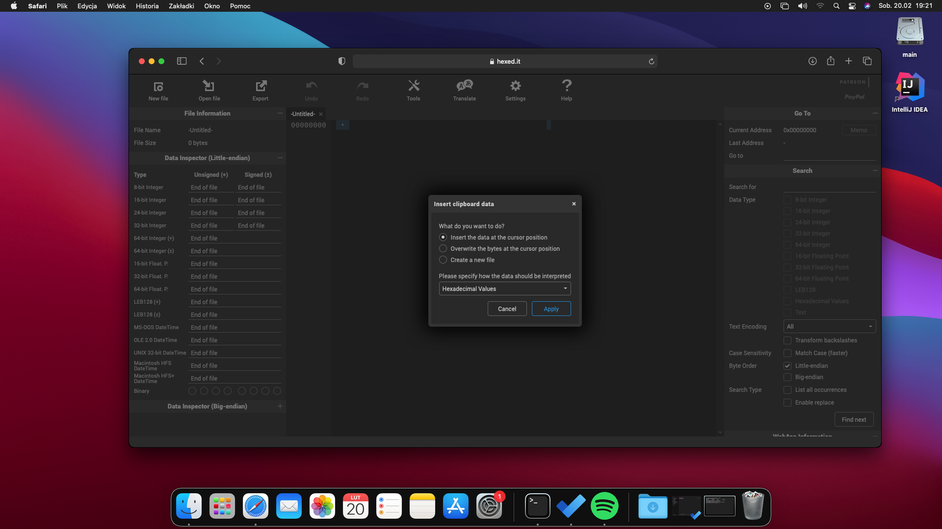
6. Our data must start with FFD8 and end with FFD9.
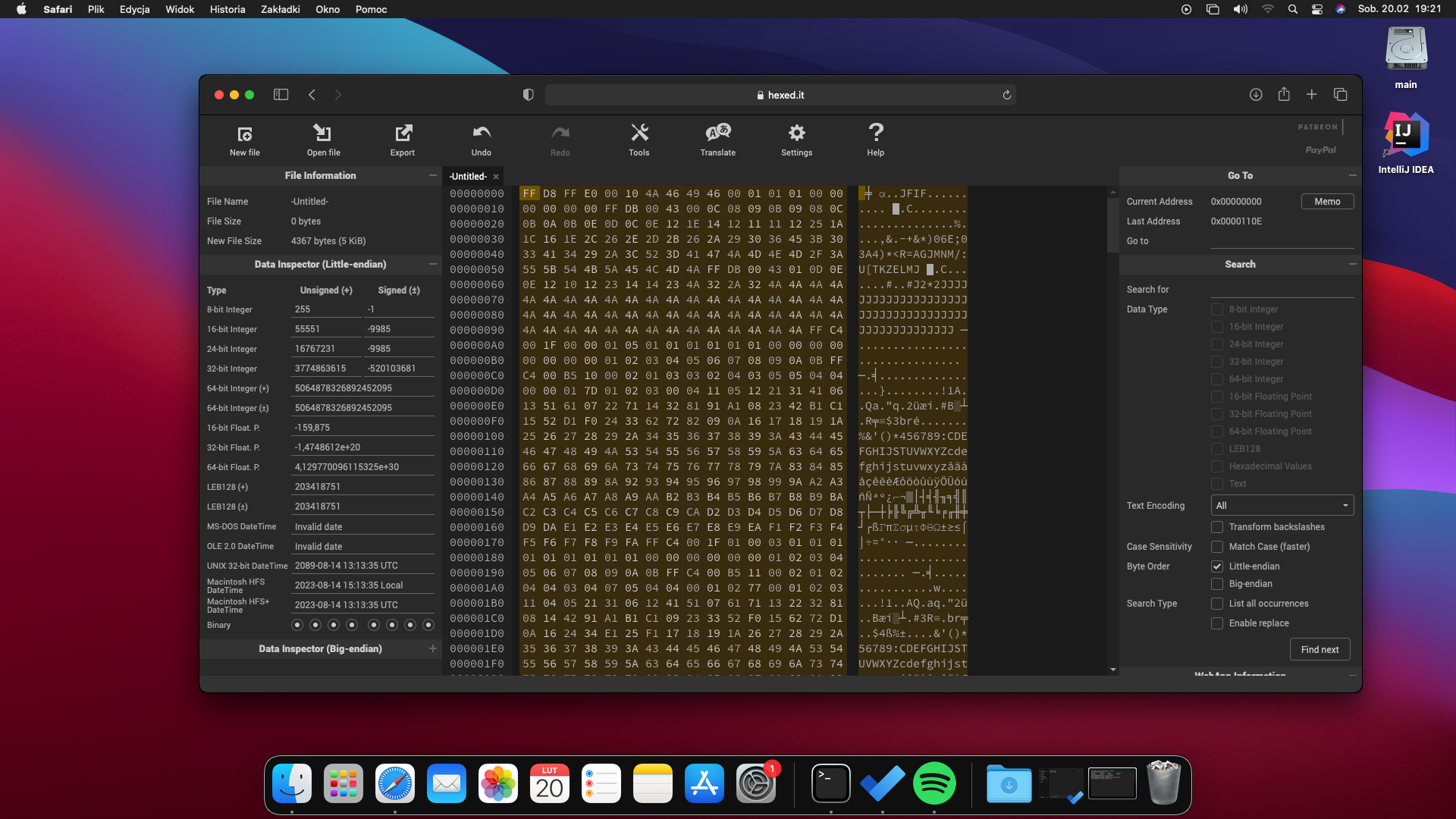
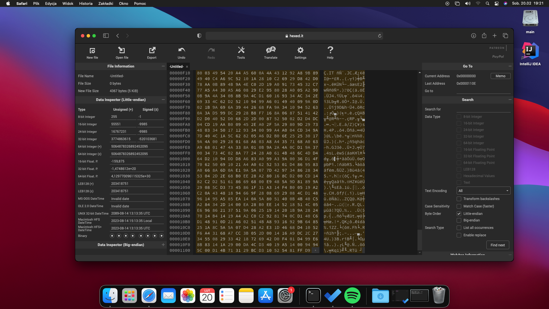
7. Save and open the newly created file.
8. Now it's all depending on you.

💀 My code doesn't work, nothing happens, what to do?
You need to make sure that:
- Using short connection wires , less than 10 cm (3.93 inches) - This is very, very, very important!,
- All wires are properly connected,
- Have a high enough clock speed for the MCU,
Use 320x240px resolution for testing - it always works :-)
Open Source Agenda is not affiliated with "STM32 OV2640" Project. README Source: SimpleMethod/STM32-OV2640
Stars
87
Open Issues
3
Last Commit
3 years ago
Repository
License