Phone Rtty Interface Save
AFSK interface for Android smartphones and tablets.
RTTY/AFSK Interface for Android Phone or Tablet
Overview
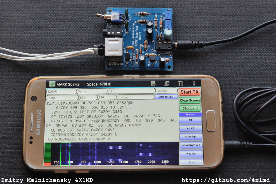
This interface board was designed for experimenting with RTTY, SSTV and other digital modes with my Yaesu FT-817ND transceiver using DroidRTTY and DroidSSTV applications on an Android phone.
Reference circuits
The idea of this circuit is not new. Many of its variants were published in the internet and the difference between them is relatively small. Usually different versions use different transistors and diodes and some resistors and capacitors values vary but the circuit remains the same.
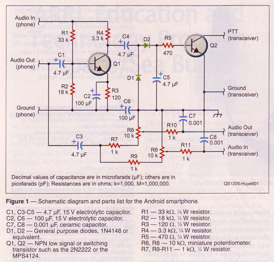
One of my sources was the article An AFSK Interface for Android Smartphones by Wolfgang Philips, W8DA, and Martin Huyett, K0BXB, which was published in the May 2012 issue of QST.
More circuits are available in links section of this document.
Revision A
The interface has two revisions. The difference between the two is relatively small. Circuit description and mechanics presented further down in this document are relevant for both revisions.
For the schematics and the photos of the first revision please refer to revision_a.md
If you got a blue PCB from me, you have the first revision board.
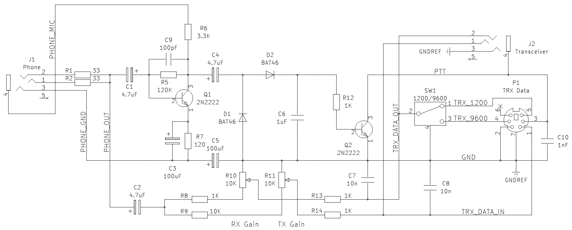
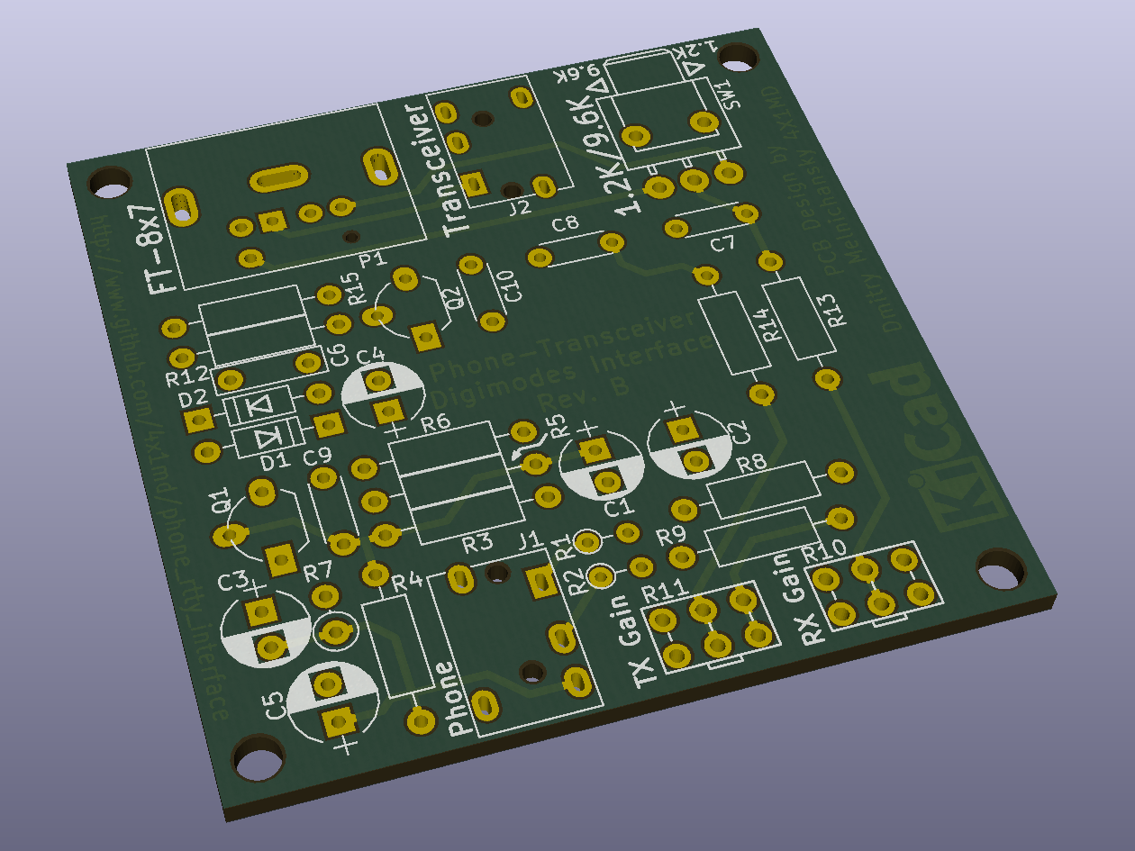
Schematic
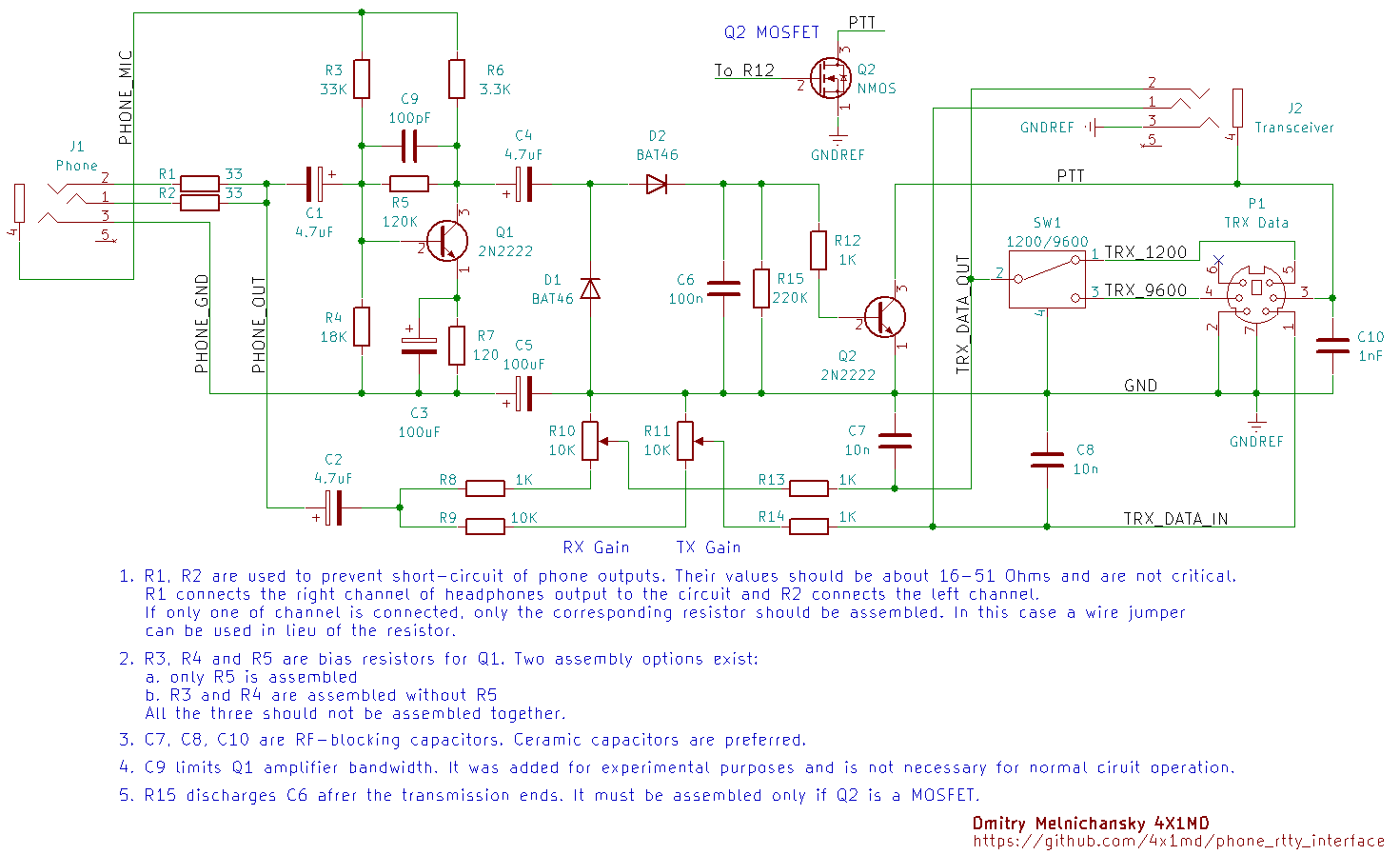
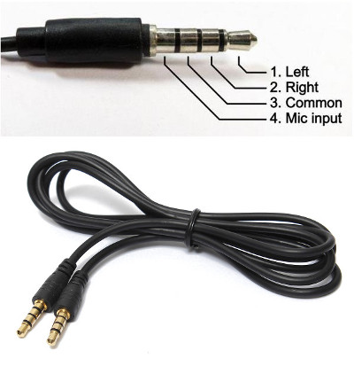
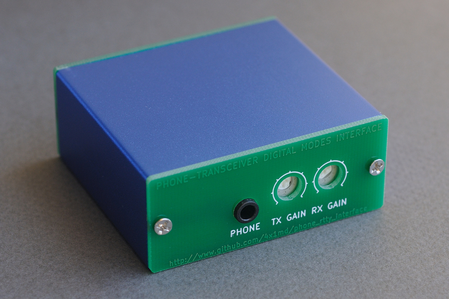
J1 connects the interface to a phone or tablet. It is a generic 4-pole 3.5mm jack. Its pinout is the same as that of Android phones. Using this jack makes connecting the phone or tablet easy requiring only a simple 3.5mm-to-3.5mm TRRS jack cable. No custom cables are required.
R1 and R2 prevent short-circuit of phone outputs. Their values are not critical and can be in the range of 10 to 51 Ohm. R1 connects the output of the right channel and R2 connects the left. One channel or both can be used. If only one channel is used, only the corresponding resistor should be assembled. In this configuration a wire jumper can be used instead of a resistor.
Transistor Q1 is a common emitter voltage amplifier stage. It is powered from the phone by the DC voltage which usually powers external microphone.
The bias resistors of this stage are R3, R4 and R5. These three resistors allow building two different amplifier types. All the three should not be assembled at the same time. Assembling R5 only creates a shunt feedback stage. In this case R3 and R4 are not required. If R3 and R4 are assembled the amplifier becomes voltage divider biased stage without AC feedback. In this case R5 is not required. These three resistor footprints leave some field for experimenting which is an essential part of the amateur radio.
Diodes D1 and D2 rectify the amplified signal and create DC bias for Q2 which pulls down the PTT line of the transceiver. Different versions of this circuit use different types of diodes. Some use silicon diodes, others use Shottkys. My assembled version worked well with 1N4148 silicon diodes. Replacing them with BAT46 Shottkys increased the rectifier output voltage. Germanium diodes like 1N34 or 1N60 should work as well in this circuit.
Transistor Q2 pulls the PTT line of the transceiver down. The PTT line of FT-817ND has pull-up resistors network with total resistance of 11 kOhm. It means that the current needed to pull the PTT voltage down to zero is 0.45 mA. It requires bias current of Q2 to be about 20 microamperes. In actual circuit the voltage on C6 will be about 0.8V which will be enough to bias Q2 into saturation.
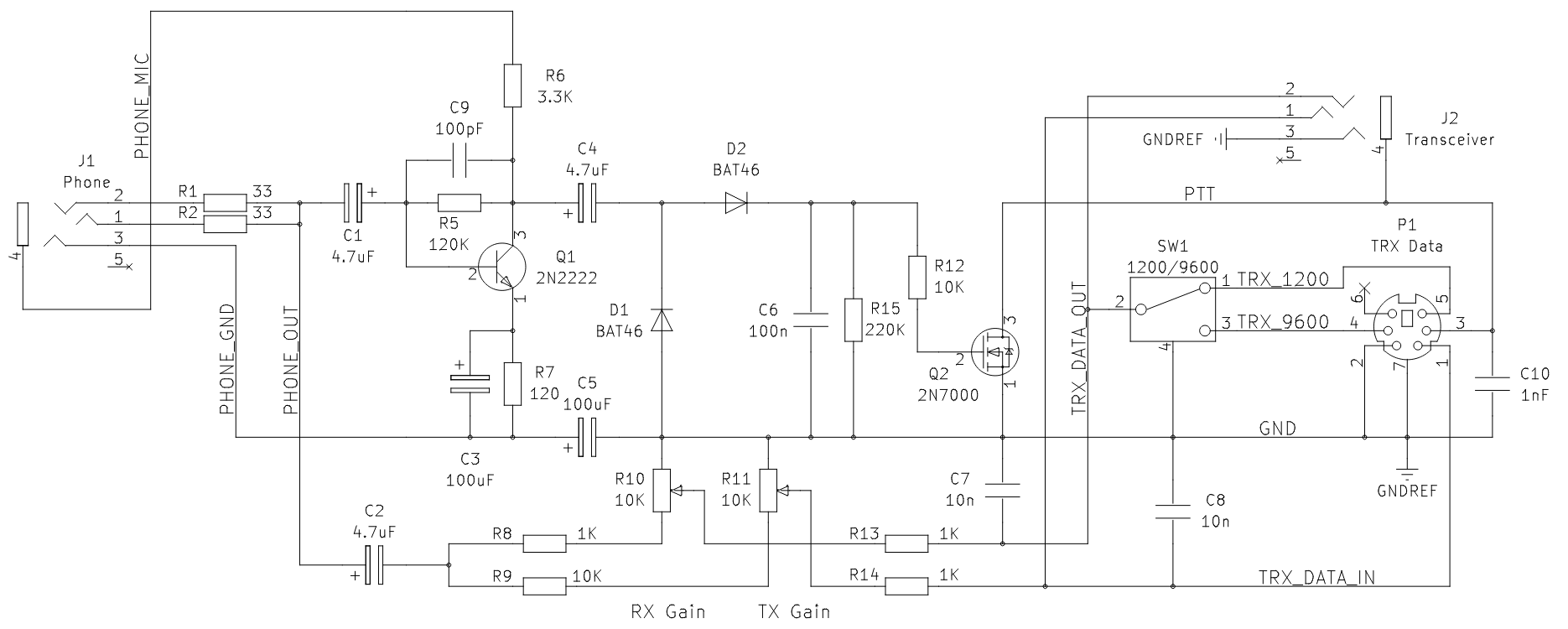
Resistor R15 discharges C6 when the PTT line needs to be released. It is required if Q2 is a MOSFET. It was added in the second version of the interface.
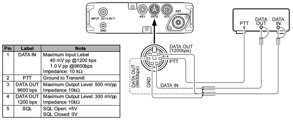
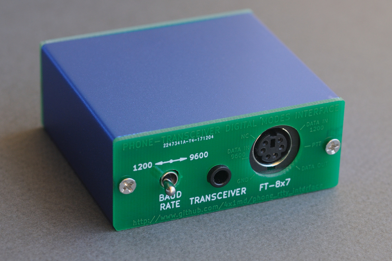
The design features two connectors for connecting a transceiver. P1 is a 6-pin mini-DIN connector which is pin-compatible with DATA connector of Yaesu FT-817. The second connector, J2 is 4-pole 3.5mm jack. It is a generic connector which can also be used to connect transceivers. The 3.5mm TRRS jack does not have PTT line. Two connectors are put for redundancy. In actual circuit only one or both can be assembled depending on requirements.
Both connectors have 1200 bps and 9600 bps lines and switch SW1 is used to choose between the two data rates. If only one data rate is required, the corresponding switch pins can be shorted with a wire jumper without assembling the switch itself.
C7 and C8 are RF-blocking capacitors thus ceramic ones are preferred. Other components are not critical. Most of them can be pulled of old electronic equipment.
Circuit analysis

If you like exploring oscilloscope output, doing some math and want more details about this circuit, please refer to circuit_description.md.
If you like simulating circuits, refer to circuit_simulations.md for LTspice simulations.
BOM variants
The second revision of the interface Q2 can be BJT or MOSFET.
BJT version
MOSFET version
The rectifier output voltage reaches approximately 2.2V when loaded with a high resistance. Therefore, a low threshold N-channel MOSFET is recommended for this circuit. For example, VN2410L has maximum Vth of 2.0V, which makes it a good choice. However, a general purpose MOSFET with a higher Vth might work too. In my circuit I used 2N7000 which has maximum threshold of 3.0V and it works well.
If Q2 is a MOSFET, R15 is require for discharging C6. Without R15, C6 will remain charged after the first transmit and the PTT line will never be released.
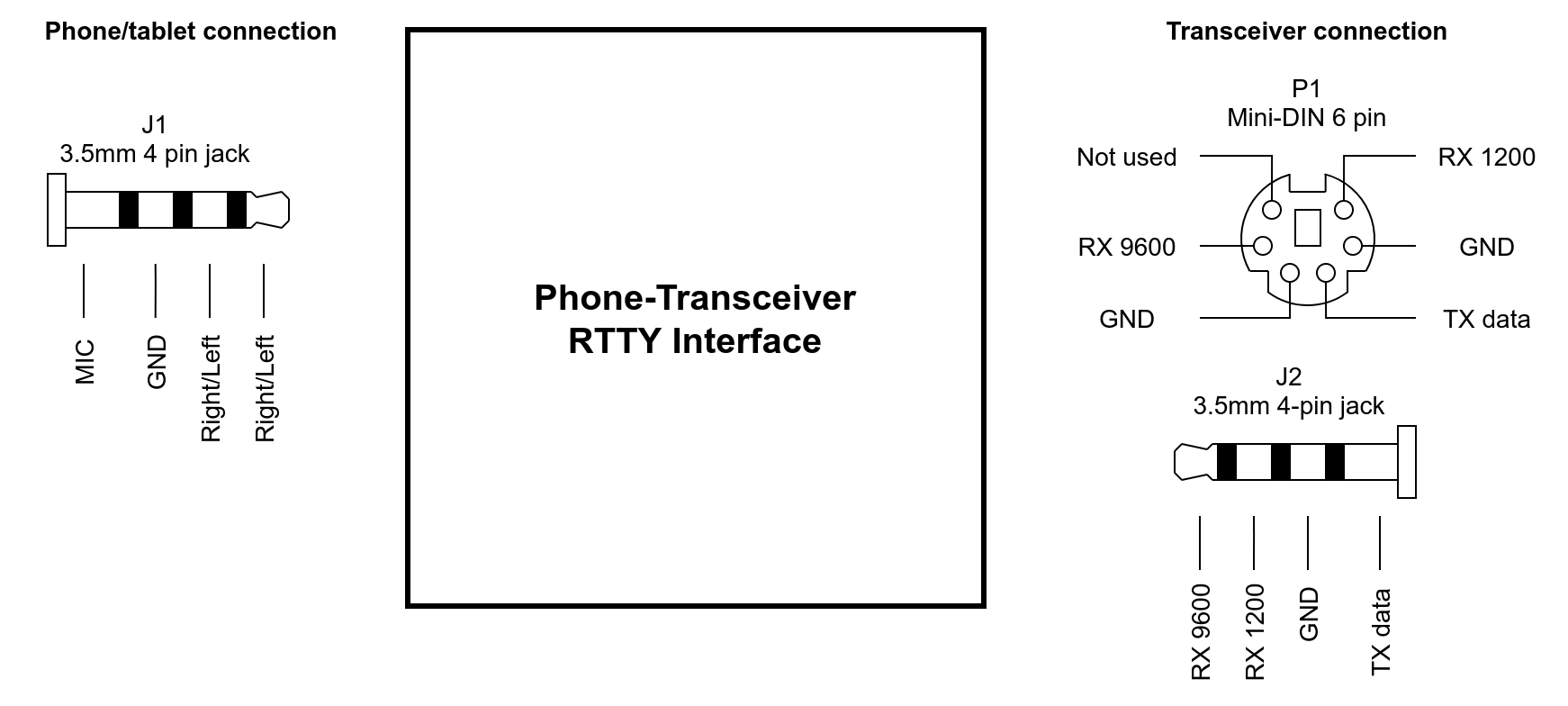
Connectors pinout
The following diagram shows the pinout of the external connectors. The phone is connected using 3.5mm jack J1. The transceiver can be connected to the 6-pin Mini-DIN connector P1 or to the 3.5mm jack J2. Connectors P1 and J2 are electrically connected. The PTT line is connected to P1 only.
Design
Requirements and considerations
- Enclosure box.
- Small size.
- Easy-to-get parts.
- Adjusting potentiometers from front or rear panel.
- No proprietary connectors.
- Easy assembly.
- Good repeatability by other hams.
- Options for experiments.
Mechanics
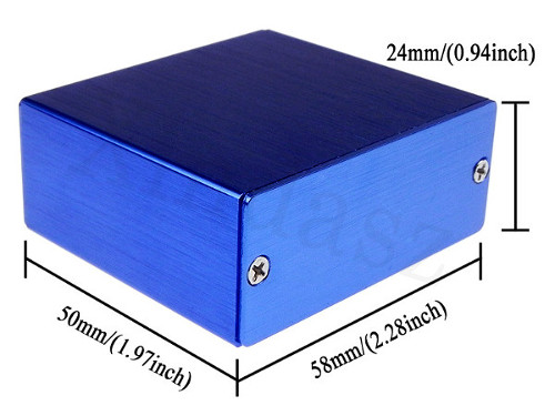
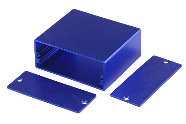
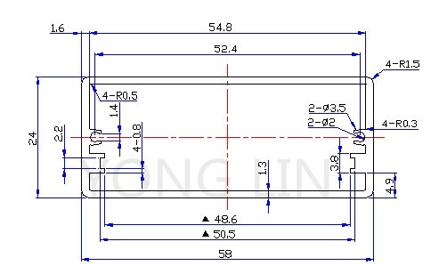
When I started the development, I decided to assemble the device in an enclosure box. The box had to be inexpensive and easily available from different electronic parts suppliers.
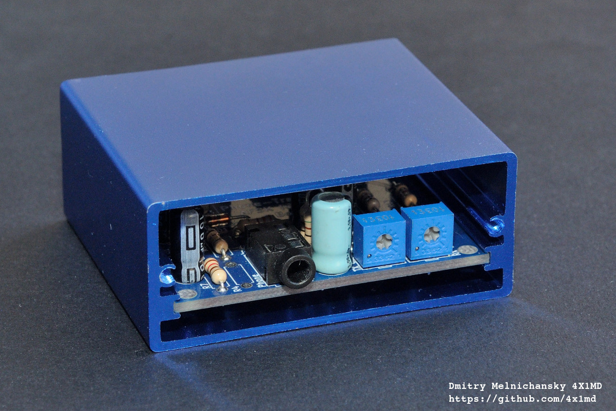
After some search I found a blue aluminium box 58x50x24mm. The box is relatively cheap and can be purchased from many sellers on eBay or AliExpress. The box fits a PCB of 50x50mm which is enough for this project and has front and rear panels which can be modified by drilling or cutting. In order to eliminate the drilling process, in revision B I created front and rear panels from PCBs.
PCB development
The PCB was designed using KiCAD software as a simple two-layer board with through-hole mounted parts.
Front and rear panels
Both front and rear panels were made from PCBs. Their fuction is mechanical only and no electronic parts are assembled on these PCBs.
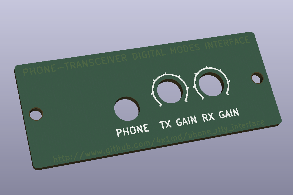
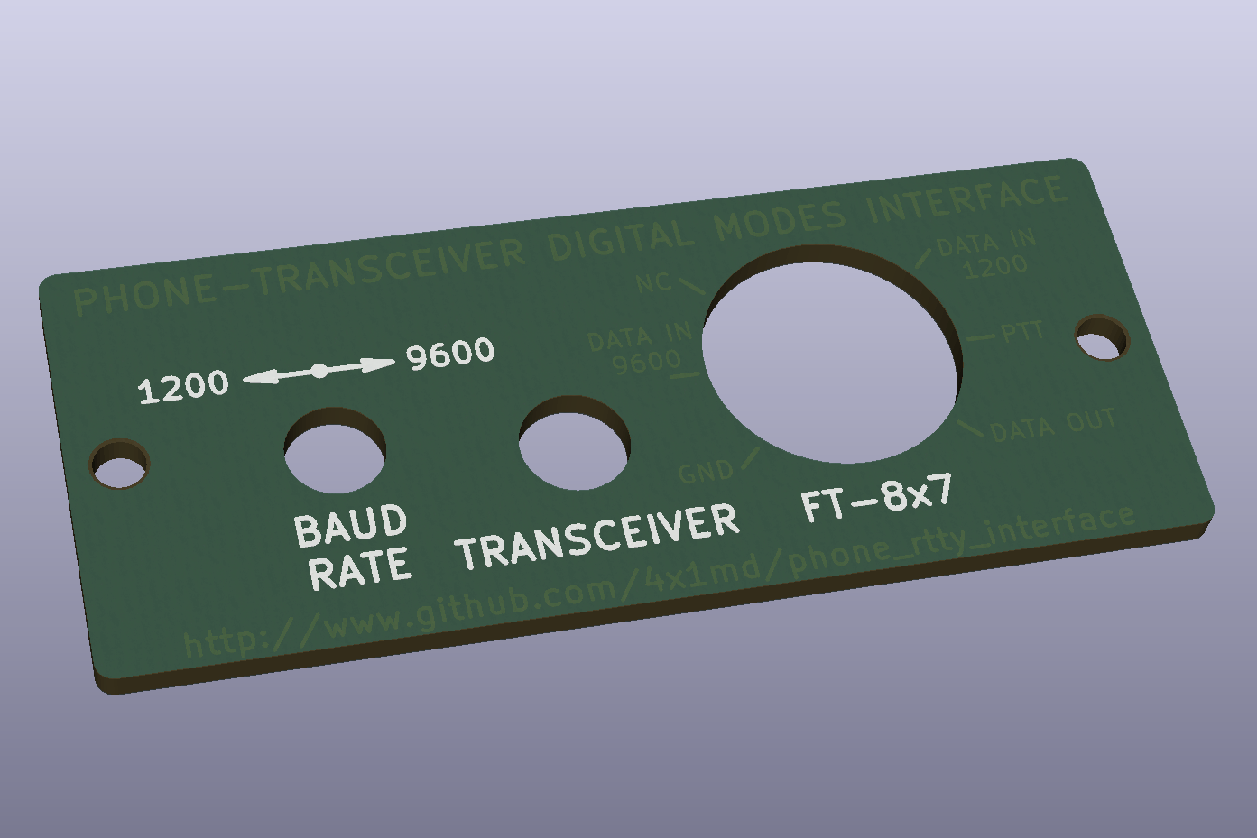
Photo gallery
Factory-produced PCB
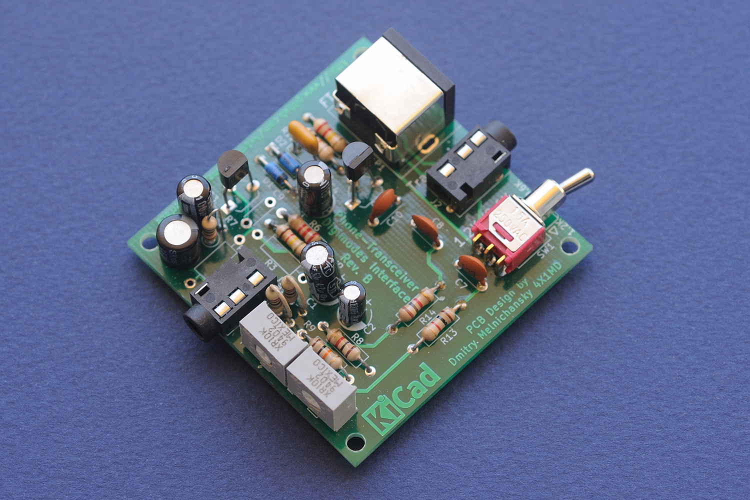
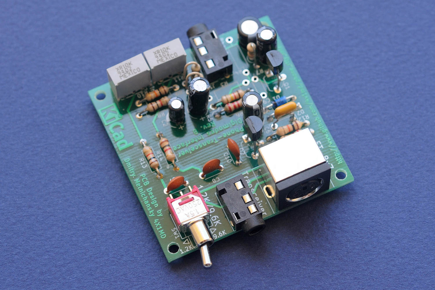
The PCBs were produced by PCBWay who did a great job. Solder mask of the first revision was made blue in order to match the color of the enclosure box. The second revision was produced with green solder mask.
:warning: Important Note! Minimum order at the factory was 10 boards from which I need only two or three. As of April 15, 2020, I have board sets (main PCB, front and rear panel), which I can give away. If you'd like to build this device for yourself, I can send you a board. Feel free to contact me.
Populated PCB
The design uses through hole parts which make PCB assembly quite simple. Connectors, trimmer potentiometers and switch are new. All the other components were recovered from old electronic equipment.
Assembled device
I haven't yet completed drilling the front and the rear panel of the box, so the device isn't yet fully assembled. The following photos show that the PCB perfectly fits in the chosen box.
The complete device with front and rear panel assembled:
Field tests and using the device
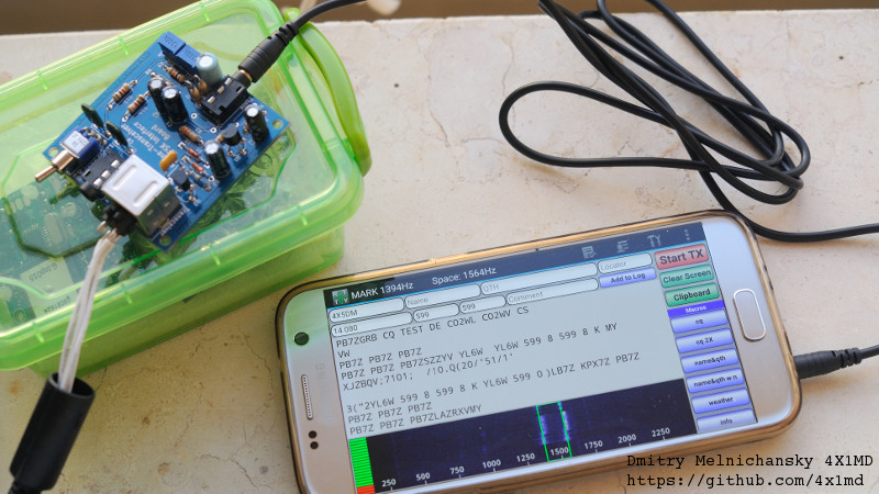
Cuba to Israel. Nice DX!
Known issues
The developers of Wolphi-Link interface report the following issue:
WolphiLink might not work properly if you transmit on VHF or UHF while having your antenna to close to your phone/tablet and WolphiLink. The PTT might get triggered by RF and would not release.
I experienced the same behavior on VHF and UHF bands especially when trying to transmit in AM, FM or PKT modes. When the transmitting antenna is close to the board the transceiver remains in TX mode and the only way to release it is to turn it off. The issue usually disappears when the phone is disconnected even if its cable is still connected to the jack.
I suppose that the cables between the transceiver and the phone become a counterpoise of the transmitting antenna and the generated RF causes transceiver keying. I don't know if this issue exists with other transceivers.
Till now, I couldn't find any solution. On HF bands and when the transmitting antenna is far from the transceiver the device functions properly.
Update: After connecting a shielded cable between the transceiver and the interface, the problem is almost completely.
Adjustments
A properly assembled device should require only RX and TX level adjustments using R10 and R11 trimmer potentiometers.
Plans for future development
If I ever do another revision of this board, I'd like to make the following improvements:
- Adding an RF-blocking capacitor to the PTT line.
- Adding PTT line to J2 3.5mm jack.
- Adding a capacitor in parallel to R5 for limiting the bandwidth of the amplifier.
- Removing ground conductor from the component layer.
- Improving the thermal relief on the grounded pads. Today they are sometimes hard to solder.
- Increasing the space between R10 and R11 to fit larger trimmer resistors.
- Adding a TX inhibit switch which will disable triggering the PTT line. It may be useful to prevent notifications or other non radio-related sounds to key the transceiver.
Links
- Designing a Phone/Radio interface: Part 1, Part 2, Part 3
- http://www.darc-husum.de/android-interface.html
- https://www.dk9jc.de/blog/equipment/109-ft-817-smartphone-interface-for-pskdroid-and-aprsdroid
- DroidSSTV manual
- Wolphi-Link interface
- http://161wt001.blogspot.com/2013/11/construction-interface-sstv-psk-rtty.html
- https://oe6fte.com/wolphilink-android-interface/
- https://g4fre.blogspot.com/2014/02/rtty-and-psk31-transceive-with-nexus-7.html
- http://wa8lmf.net/ham/tonekeyer.htm
- https://9m2pju.blogspot.com/2012/05/droidpsk-psk-on-your-android-phone.html
- Enclosure box: http://www.ebay.com/itm/171186884639
Questions? Suggestions?
You are more than welcome to contact me with any questions, suggestions or propositions regarding this project. You can:
- Visit my QRZ.COM page
- Visit my Facebook profile
- Write me an email to iosaaris =at= gmail dot com
How to Support or Say Thanks
If you like this project, or found here some useful information and want to say thanks, or encourage me to do more, you can buy me a coffee!


You can aslo make a donation with PayPal:

73 de 4X1MD