HDLab FPGA Development Board Save
Open source FPGA development platform
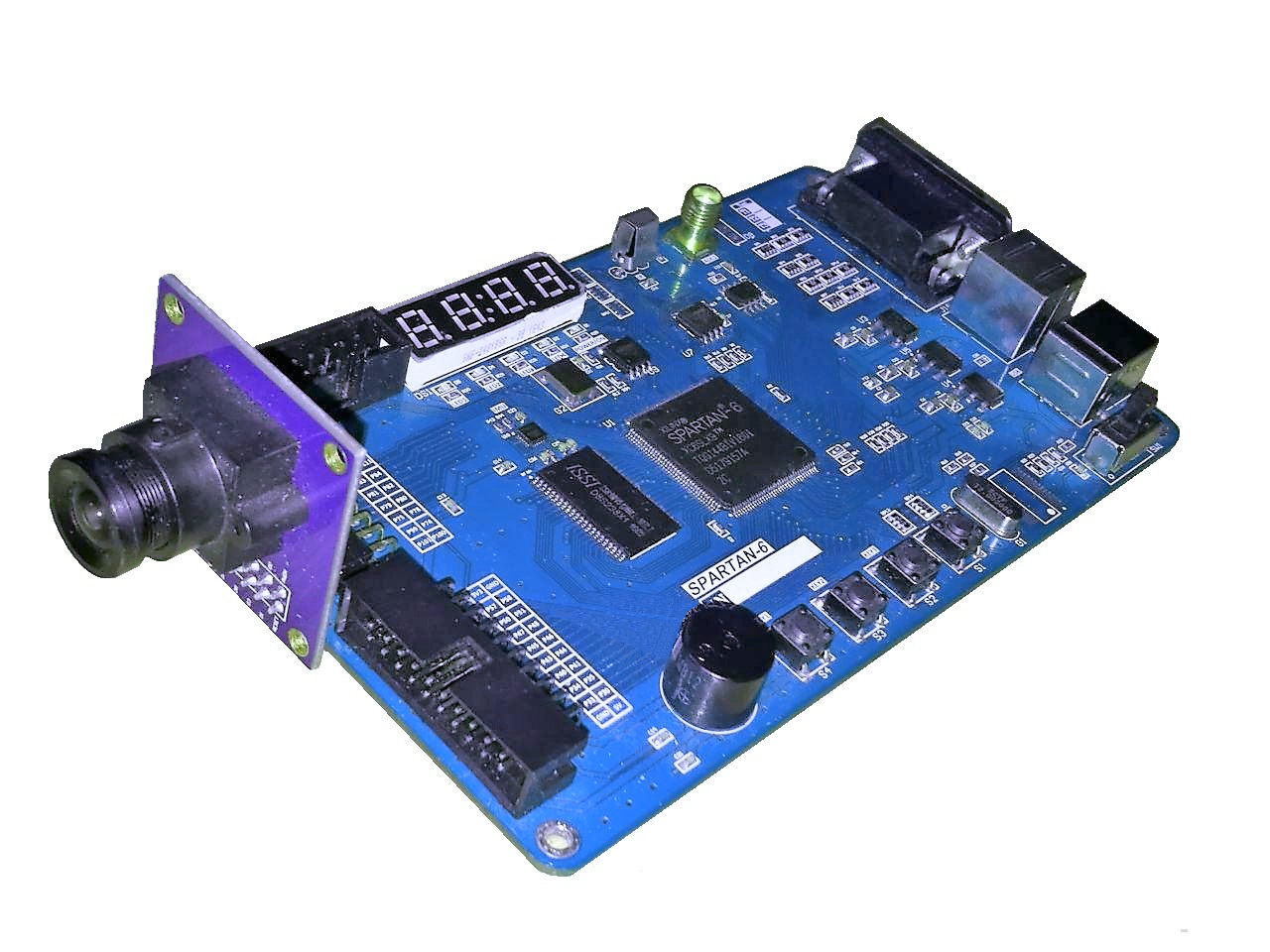
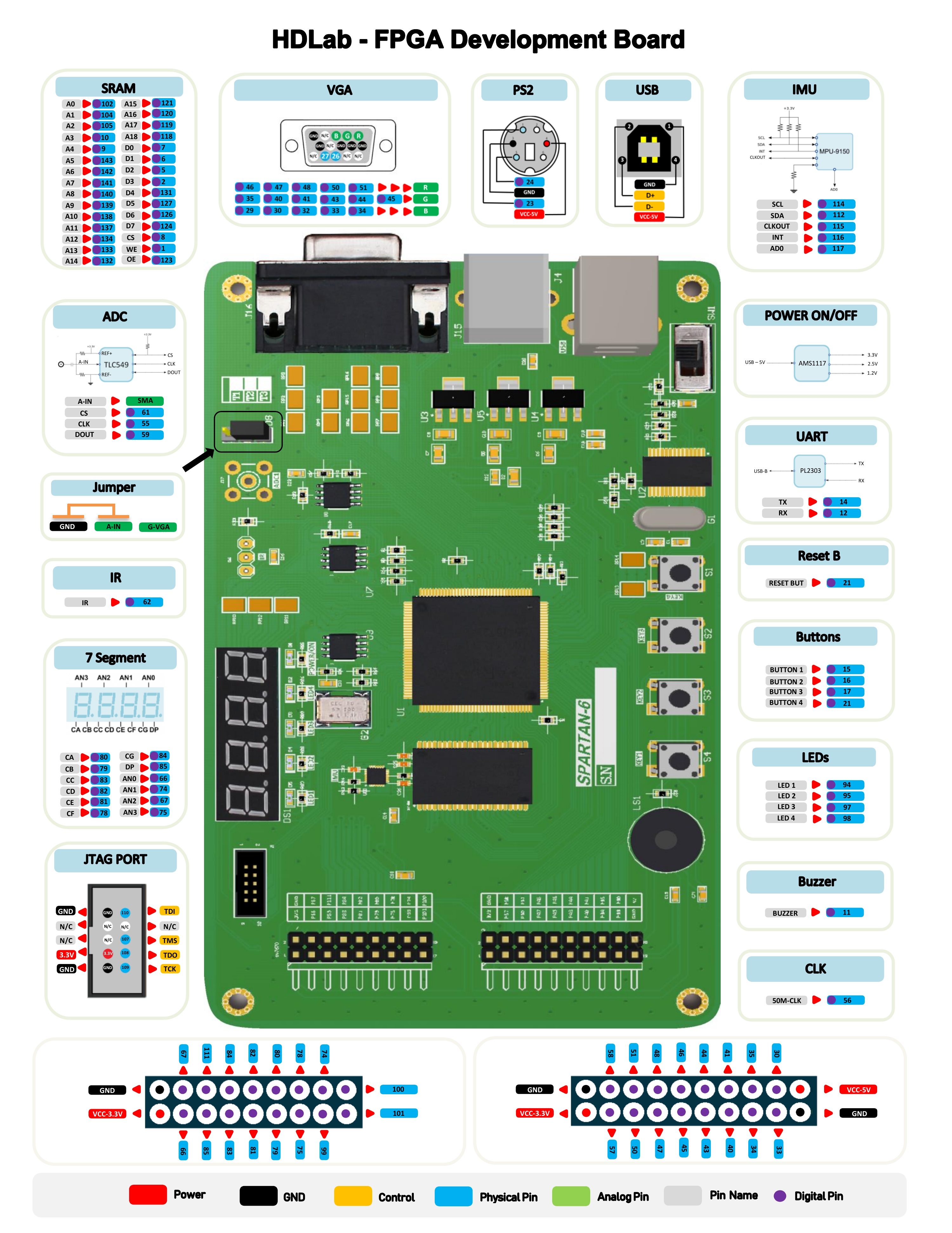
HDLab – FPGA Development Board
HDLab is an FPGA development board that provides a rich set of features and capabilities for experimenting with digital system design using FPGAs. Designed with learners and experimenters in mind, HDLab is an ideal platform for exploring the potential of FPGAs and gaining hands-on experience with digital system design.
Featuring a powerful FPGA chip, HDLab provides ample resources for implementing complex digital circuits and systems. The board also includes a range of peripherals and interfaces, including LEDs, switches, buttons, UART, VGA, and camera, to enable a broad range of experiments and projects.
HDLab comes with comprehensive documentation, tutorials, and example projects to help you get started quickly and easily. Whether you are a student, hobbyist, or professional, HDLab is a versatile and powerful tool for learning and experimentation in digital system design.
This project is used in several educational centers...
Features
-
FPGA:
- Xilinx FPGA Spartan-6 [XC6SLX9-2TQG144C]
-
Memory:
- 512-K x8 SRAM(4 M-bit) [IS61WV5128BLL]
- 128M-bit Serial Flash Memory [W25Q128FVSG]
- 32M-bit Serial Config Flash [W25Q32FVS1G]
-
Control & I/O:
- 1x Camera Interface / Camera Module [CMOS-OV7670]
- 1x IMU / 9 degrees of freedom IMU [MPU-9150]
- 1x 4 digit seven segment displays
- 4x General Purpose LEDs
- 4x General Purpose Button (1x Reset Button)
- 1x IR Interface
- 1x Buzzer
- 1x Crystal oscillator 50-Mhz
- 1x SMA Connector for ADC
- 32x GPIO 16)x GPIO for Camera Module)
-
Interface:
- 1 x USB Type-B / USB to Serial Converter [PL-2303]
- 1 x VGA / 16-bit true color of RGB565 mode
- 1 x PS2 / Standard PS2 Interface
- 1 x JTAG 10PIN / JTAG Download Debug Interface
- RS232
-
Convertor:
- 1CH ADC 1M/8bit [TLC549C]
-
Other:
- 1 x ON/OFF switch
- 1 x LED to Show Power Connection
- Operating Voltage 5-9V
- Dimensions : 8cm x 14cm
Applications
- Learning Digital Electronics
- Educational tool for schools and universities
- Robotics
- Internet of Things (IoT)
- Signal Processing
- Embedded systems
- Image Processing
- Product Prototyping
What other tools do you need?
- A text editor (for example Notepad++)
- Xilinx ISE Software (Download)
- USB JTAG Programmer for Xilinx FPGA
License
Free Hardware and Software!
More Information:
What is FPGA?
Software is the basis of all applications. Whether for entertainment, gaming, communications, or medicine, many of the products people use today began as a software model or prototype. Based on the performance and programmability constraints of the system, the software engineer is tasked with determining the best implementation platform to get a project to market. To accomplish this task, the software engineer is aided by both programming techniques and a variety of hardware processing platforms. On the programming side, previous decades yielded advances in object-oriented programming for code reuse and parallel computing paradigms for boosting algorithm performance. The advancements in programming languages, frameworks, and tools allowed the software engineer to quickly prototype and test different approaches to solve a particular problem. This need to quickly prototype a solution leads to two interesting questions. The first question of how to analyze and quantify one algorithm against another is extensively discussed in other works. The second question of where to execute the algorithm is addressed in this guide in relation to field programmable gate arrays (FPGAs). Regarding where to run an algorithm, there is an increasing focus on parallelization and concurrency. Although the interest in the parallel and concurrent execution of software programs is not new, the renewed and increased interest is aided by certain trends in processor and application-specific integrated circuit (ASIC) design. In the past, the software engineer faced two choices for getting more performance out of a software algorithm: a custom-integrated circuit or an FPGA. The first and most expensive option is to turn the algorithm over to a hardware engineer for a custom circuit implementation. The cost of this option is based on:
- Cost to fabricate the circuit
- Time to translate the algorithm into hardware
Despite advancements in fabrication process node technology that have yielded significant improvements in power consumption, computational throughput, and logic density, the cost to fabricate a custom-integrated circuit or ASIC for an application is still high. At each processing node, the cost of fabrication continues to increase to the point where this approach is only economically viable for applications that ship in the range of millions of units. The second option is to use an FPGA, which addresses the cost issues inherent in ASIC fabrication. FPGAs allow the designer to create a custom circuit implementation of an algorithm using an off-the-shelf component composed of basic programmable logic elements. This platform offers the power consumption savings and performance benefits of smaller fabrication nodes without incurring the cost and complexity of an ASIC development effort. Similar to an ASIC, an algorithm implemented in an FPGA benefits from the inherent parallel nature of a custom circuit. Reference & Learn More
FPGA Programming Model
The programming model of a hardware platform is one of the driving factors behind itsadoption. Software algorithms are typically captured in C/C++ or some other high-levellanguage, which abstracts the details of the computing platform. These languages allow forquick iteration, incremental improvements, and code portability, which are critical to thesoftware engineer. For the past few decades, the fast execution of algorithms captured inthese languages have fueled the development of processors and software compilers.Initially, improving the runtime of software was based on two central concepts: increasingprocessor clock frequency and using specialized processors. For many years, it was commonpractice to wait a year for the next generation processor as a way to speed up execution. Atevery new higher clock frequency, the software program ran faster. Although this wasacceptable in some cases, for a large set of applications, incremental speedup throughprocessor clock frequency is not enough to deliver a viable product to market.For this type of application, the specialized processor was created. Although there are many kinds of specialized processors, such as the digital signal processor (DSP) and graphics processing unit (GPU), all of these processors are capable of executing an algorithm written in a high-level language, such as C, and have function-specific accelerators to improve the execution of their target software applications. With the recent paradigm shift in the design of standard and specialized processors, both types of processors stopped relying on clock frequency increases for program speedup and added more processing cores per chip. Multicore processors put program parallelization at the forefront of techniques used to boost software performance. The software engineer must now structure algorithms in a way that leads to efficient parallelization for performance. The techniques required in algorithm design use the same base elements of FPGA design. The main difference between an FPGA and a processor is the programming model.Historically, the programming model of an FPGA was centered on register-transfer level (RTL) descriptions instead of C/C++. Although this model of design capture is completely compatible with ASIC design, it is analogous to assembly language programming in software engineering. Reference & Learn More
What is VHDL?
VHDL is a hardware description language. It describes the behavior of an electronic circuit or system, from which the physical circuit or system can then be attained (implemented).VHDL stands for VHSIC Hardware Description Language. VHSIC is itself an abbreviation for Very High Speed Integrated Circuits, an initiative funded by the United States Department of Defense in the 1980s that led to the creation of VHDL. Its first version was VHDL 87, later upgraded to the so-called VHDL 93. VHDL was the original and first hardware description language to be standardized by the Institute of Electrical and Electronics Engineers, through the IEEE 1076 standard. An additional standard, the IEEE 1164, was later added to introduce a multi-valued logic system [1].
VHDL is intended for circuit synthesis as well as circuit simulation. However, though VHDL is fully simulatable, not all constructs are synthesizable [1].
A fundamental motivation to use VHDL (or its competitor, Verilog) is that VHDL is a standard, technology/vendor independent language, and is therefore portable and reusable. The two main immediate applications of VHDL are in the field of Programmable Logic Devices (including CPLDs—Complex Programmable Logic Devices and FPGAs—Field Programmable Gate Arrays) and in the field of ASICs (Application Specific Integrated Circuits). Once the VHDL code has been written, it can be used either to implement the circuit in a programmable device (from Altera, Xilinx, Atmel, etc.) or can be submitted to a foundry for fabrication of an ASIC chip. Currently, many complex commercial chips (microcontrollers, for example) are designed using such an approach [1]. Reference & Learn More